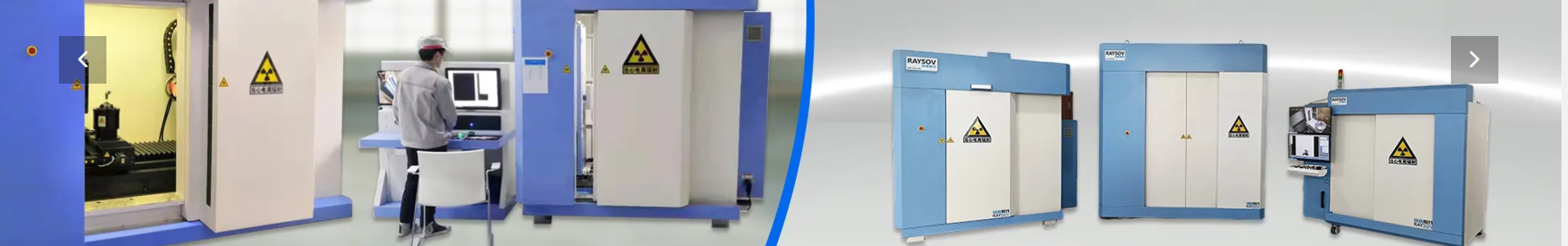
X-ray semiconductor, SMT, and electron/electric components CT Scan Solutions
3D X-ray computed tomography (CT) is a non-destructive testing (NDT) technology, which rebuilt the internal structure of objects in 3D images.
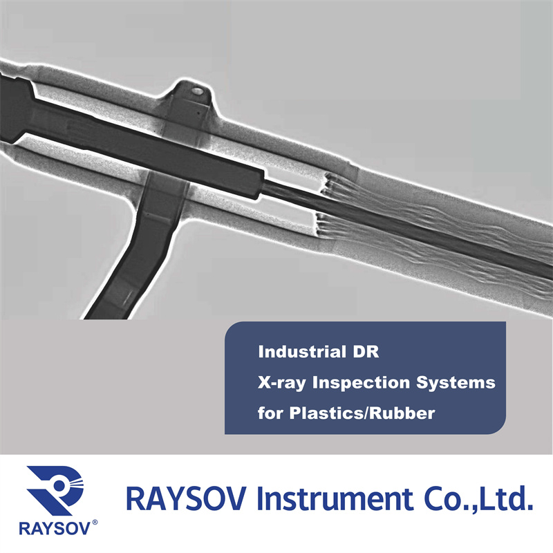
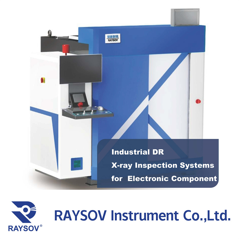
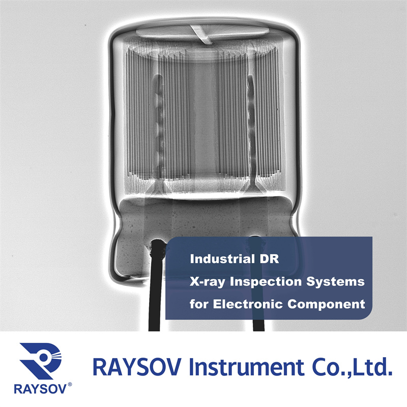
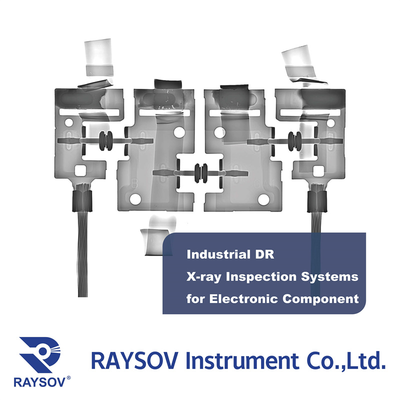
X-ray Printed Circuit Board(PCB)semiconductor, SMT, and electron/electric components CT Scan Solutions,base on advanced 3D CT inspection system used for applications including PCBs. Internal structures and defects including BGA Short, Bridging, Open, De-wet, Void, Poor Hole Filling can be identified and measured.
semiconductor, SMT, and electron/electric components industry has been an important and irreplaceable industry in modern production and life of human beings.With the continuous improvement of economic level and industrial automation, the demand for PCBs is growing exponentially and explosively, and the value of semiconductor, SMT, and electron/electric components radiates to all walks of life.
X-ray Hydrogen storage tank CT scaning Solutions
X-ray Foundry Casting CT scan Solutions
X-ray Fiber Composite Material CT scan Solutions
X-ray Batteries CT scan Solutions
X-ray Wheel Hub CT scan Solutions
Additive Manufacturing(AM) Component CT Inspection Systems
X-ray Defense Componet CT scan Solutions
Custom bulit X-ray CT can Solutions
X-ray Printed Circuit Board(PCB) CT scan Solutions